Executive Department for
Press, Communication and Marketing
Adolf-Reichwein-Straße 2a Gebäude AVZ (Gebäudeteil AR-NA) 57068 Siegen
Phone: +49 (0)271/740-4915 Fax.: +49 (0)271/740-4911 E-Mail: presse@uni-siegen.de
The Future of 3D Imaging

Faster and more precise: Scientists in the ULTRA-SENSE 3D project at the University of Siegen are exploring potentials and benchmarks of 3D image sensors based on amorphous silicon and its alloys.
Whether for the automotive industry, medical technology, security systems, or smartphones: 3D cameras represent a rapidly evolving technology with ever-widening distribution and applications. As a future-facing topic with massive societal relevance, these sensor systems have taken a central role in the work of the research groups “Graphene-Based Nanotechnology” and “High Frequency and Quantum Electronics” at the University of Siegen.
One technique whose user-friendliness has made it increasingly popular for state-of-the-art 3D camera systems is Time-of-Flight (ToF). It leverages the time difference between sending a light impulse and its back reflection from the scene to precisely determine distances and producing images with spatial depth. Yet ToF sensors are relatively complicated and demanding in terms of chip integration effort and required chip space. This drawback makes conventional ToF sensors not only expensive, but also difficult to use in scaled application fields requiring Very Large-Scale Integration (VLSI), which reflects the absolute number of light-sensitive sensors on a microchip.
In the new “ULTRA-SENSE 3D” research project, scientists at the University of Siegen are working on innovative and powerful high-precision 3D camera systems based on the Focus-Induced Photoresponse (FIP). “FIP is a quite novel technique based on intensive research efforts performed at ZESS, the Center for Sensor Systems at the University of Siegen,” explains Dr. Andreas Bablich, who leads the project together with Dr. Peter Haring Bolívar. Their research now seeks to concentrate on the potential benefits of 3D-compatible FIP sensors based on amorphous silicon. “I’m very pleased to be working on this kind of project, which demonstrates the close, fruitful collaboration between basic research and innovative impulses for industrial implementation.” Prof. Dr. Peter Haring Bolívar affirms. ULTRA-SENSE 3D been earmarked to receive almost three-quarters of a million euros in funding over three years from the German Research Foundation (DFG). For Dr. Andreas Bablich, the success of his first proposal marks an important milestone in his research career—and reflects the DFG’s stated commitment to funding early-career researchers.
Compared with other current 3D sensing concepts, FIP sensors can achieve a much better precision to identify depth information across long distances, even from just one image point (pixel). This derives from its methodology, which measures not only the amount of light striking the sensor, but also the size of the light spot, which in turn allows for precise distance measurements in real time, even when the ambient light is weak. “The problem of current FIP detector sensors and concepts that rely on organic or lead-based material is that read-out speed and sensitivity for current FIP detectors using organic or lead-based materials are massively limited,” notes Dr. Andreas Bablich. To counter this, the working groups follow a new approach using amorphous silicon (a-Si:H) FIP sensors that are capable to obtain the FIP effect at much higher operation speeds that exceed values of state-of-the art sensors by two orders of magnitude faster. In addition, a-Si:H FIP sensors are more sensitive regarding the required amount of light. A thin layer of the active material, amorphous silicon, is applied to a chip at low temperatures.
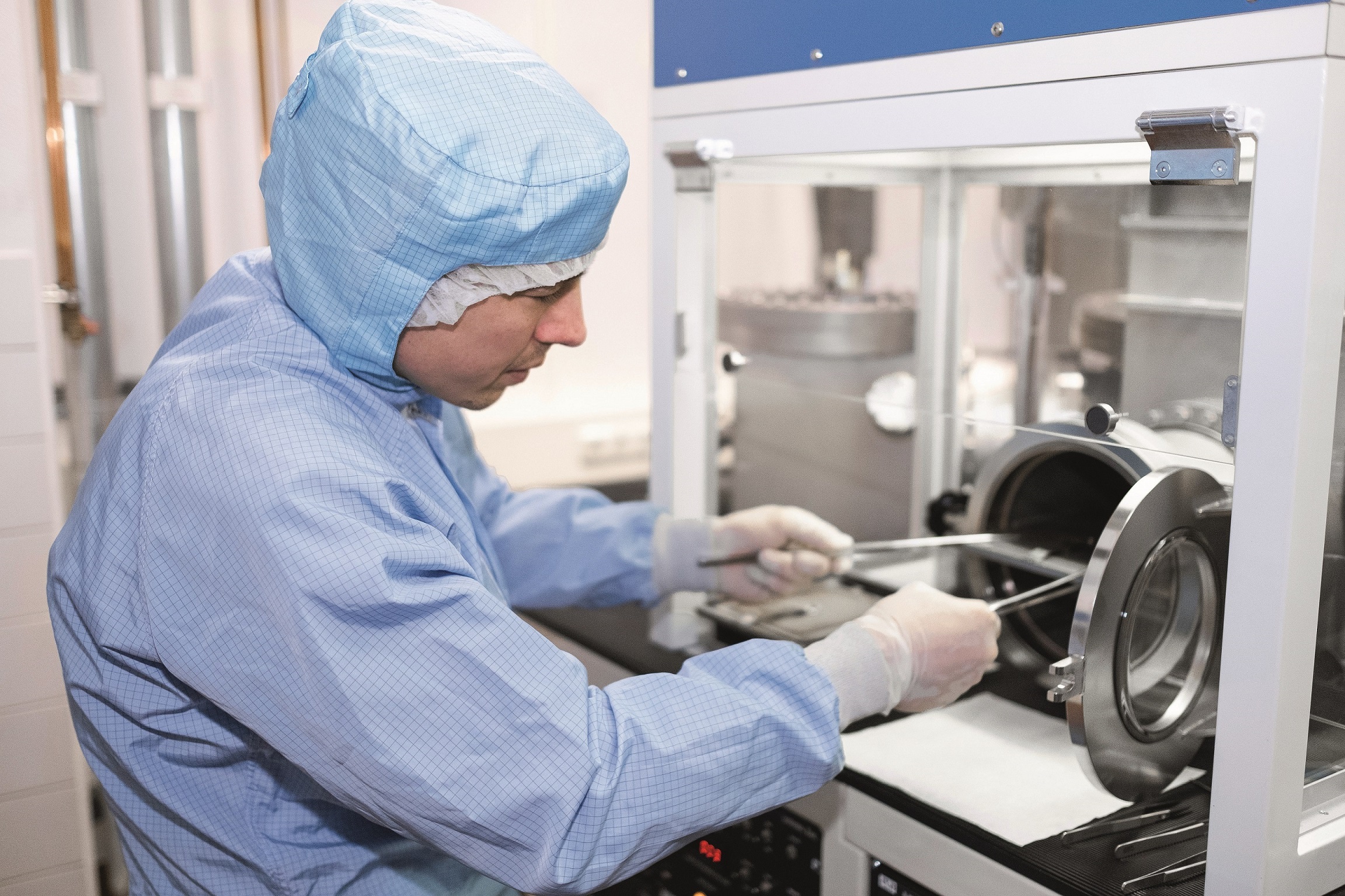
In technical lingo, the researchers are focused on plasma-enhanced chemical vapor deposition of silicon on the chip surface. Typical layer thicknesses range between 10 nanometers and 1.5 micrometers, the latter representing roughly one-hundredth the diameter of a strand of human hair. “Our work through the research groups goes beyond just developing, optimizing, and characterizing the sensor concepts here at the teaching chair; we’re also producing the sensors in the University's current clean room. We are highly excited and looking forward for the upcoming opening of the INCYTE research building including a 600m2 cleanroom and ISO-4 class at the Adolf-Reichwein campus to only further boost and intensify the technical implementation of these and other fascinating research topics.”
Beyond the sensors themselves, the scientists in Siegen have also framed an innovative readout concept to significantly raise frame rates on integrated 3D cameras and reduce noise distortion. In Dr. Bablich’s words: “An initial set of distance measurements have already been conducted and resolutions of roughly 500 micrometers achieved, showing tremendous potential for major improvements to the FIP detection process.” The researchers see one potential key application in high-sensitivity 3D scene recognition, which could be useful in automotive, security technology or industrial quality assurance.