Solid State Physics
In the Solid State Physics research group, ultra-thin 2D materials are prepared and characterized using surface research methods. Starting with the prototypical graphene (Nobel Prize in Physics 2010), which consists of a monoatomic layer of carbon, numerous other members of this class of materials have been discovered in recent years, enabling 2D materials to establish themselves as a field of research in their own right.
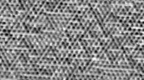
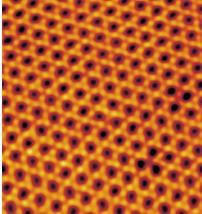
Our main method of investigation is scanning tunneling microscopy (STM), which can achieve atomic resolution. We prepare advanced 2D materials such as composites of ultra-thin semiconductors or two-dimensional ferroelectric materials under precisely controlled conditions and modify these layers in a targeted manner, e.g. to induce doping or to investigate the interaction with potentially interfering gases. In recent years, we have been able to show that an ultra-thin diode can be produced from MoS2 and WS2 and have developed a preparation method for 2D ferroelectrics.


Our research profile
The Solid State Physics group prepares and characterizes ultrathin 2D materials using surface research methods. Starting with the prototypical graphene (Nobel Prize in Physics 2010), which consists of a monoatomic layer of carbon, numerous other members of this class of materials have been discovered in recent years. Theoretically, several hundred different materials are possible, but only very few of them have already been synthesized.
Our main method of investigation is scanning tunneling microscopy (STM), with which atomic resolution can be achieved. We prepare advanced 2D materials such as composites of graphene and hexagonal boron nitride or ultrathin semiconductors such as MoS2 under precisely controlled conditions and modify these layers in a targeted manner, e.g. to induce doping or to investigate the interaction with potentially interfering gases from the environment. In recent years, we have been able to show that electrons can be trapped in quantum dots of graphene, how graphene is damaged when shot with energetic ions, and how it manages to creep between 2D materials and their substrate (intercalation).
Main research areas
- Ultra-thin 2D materials
- Methods of surface research
- Preparation and characterization
- Scanning tunneling microscopy (STM)
Publications
Kirkendall Voids in Monolayer MoxTayS2 Alloys on Au(111)
Kirkendall Voids in Monolayer MoxTayS2 Alloys on Au(111)
Transition from fractal-dendritic to compact islands for the 2D-ferroelectric SnSe on graphene/Ir(111)
Transition from fractal-dendritic to compact islands for the 2D-ferroelectric SnSe on graphene/Ir(111)
Probing the interplay of interactions, screening and strain in monolayer MoS2 via self-intercalation
Probing the interplay of interactions, screening and strain in monolayer MoS2 via self-intercalation
What governs the atomic structure of the interface between 2D transition metal dichalcogenides in lateral heterostructures?
What governs the atomic structure of the interface between 2D transition metal dichalcogenides in lateral heterostructures?
Dislocation-free two-dimensional concentric lateral heterostructures: MoS2–TaS2/Au(111)
Dislocation-free two-dimensional concentric lateral heterostructures: MoS2–TaS2/Au(111)
Tin Halide Perovskite Epitaxial Films on Gold Surfaces: Atomic Structure and Stability
Tin Halide Perovskite Epitaxial Films on Gold Surfaces: Atomic Structure and Stability
Nucleation Stage for the Oriented Growth of Tantalum Sulfide Monolayers on Au(111)
Nucleation Stage for the Oriented Growth of Tantalum Sulfide Monolayers on Au(111)
Phase engineering in tantalum sulfide monolayers on Au(111)
Phase engineering in tantalum sulfide monolayers on Au(111)
Spatial variation of geometry, binding, and electronic properties in the moiré superstructure of MoS2 on Au(111)
Spatial variation of geometry, binding, and electronic properties in the moiré superstructure of MoS2 on Au(111)
Metal-insulator transition in monolayer MoS2 via contactless chemical doping
Metal-insulator transition in monolayer MoS2 via contactless chemical doping
Sub-Poissonian distribution of Cs and K ions in the valleys of
hBN/Ru(0001)
Sub-Poissonian distribution of Cs and K ions in the valleys of
hBN/Ru(0001)
Structure of monolayer TaS2 on Au(111)
Structure of monolayer TaS2 on Au(111)
Open Projects
Topics for Bachelor's and Master's theses
Preparation of two-dimensional germanium selenide (GeSe)
GeSe is a novel 2D material with potential applications in ultra-small data storage devices due to its ferroelectric properties. We observe that the structure of this material depends very sensitively on the preparation conditions, especially the growth temperature. In this project, the preparation will therefore be perfected and partially automated in order to fully explore the phase diagram.
Investigation of the insect skin using AFM

In simple terms, the cuticle is the skin of insects. It consists of chitin and proteins and, in addition to its protective function, has other sensory and movement functions. Using the example of a fly's eye, we were recently able to show that our AFM is suitable for imaging such biological systems. This is to be further developed in this project. Among other things,wax layers on beetle wingscanbe investigated with regard to structure and frictional propertiesin
collaboration with the Merzendorfer group (Molecular Physiology).
Kagome structure
The Kagome lattice has interesting electronic and magnetic properties that are being intensively studied, particularly in theory. However, experimental realizations, especially for two-dimensional materials, are still rare. We have recently found such a material, consisting of Ta and S atoms on a gold surface. The aim of this bachelor thesis is to improve the preparation of the Kagome structure so that the structure and properties can be analyzed unambiguously.
Ultra-thin Janus membranes
Janus membranes are films that have different properties on opposite sides. The ultimate Janus membranes are 2D
materials that can exhibit contrasting characteristics in a very small space. The different atoms on both sides create a built-in electric field, which also makes these materials interesting for photovoltaics. We have developed a promising new process for producing such membranes, which is now to be implemented in practice in this master's thesis.
Controlled preparation of tips for scanning tunneling microscopy
Scanning tunneling microscopy (STM) allows the characterization of surfaces on the atomic scale. The tip of the STM is the most important and most delicate part, and its preparation is crucial for all measurements. In this project, an existing setup for
tip preparation will be optimized with the goal of a routine fabrication of reliable tips for our ultra-high vacuum microscopes.
Optimizing the preparation of ultrathin materials

Transition metal dichalcogenides are an important subgroup of 2D materials. We prepare them under highly controlled conditions using Molecular Beam
Epitaxy (MBE). This project focuses on fine-tuning growth conditions, leveraging control electronics, implementing feedback loops, and advancing automation. You will work hands-on with state-of-the-art tools to optimize the growth process.
2D materials workshop for the physics study day
Every year, the Department of Physics offers a study day where high school students interested in physics can find out about our research topics. In this project, a workshop will be developed in which the research field of two-dimensional materials
can be discovered.
Scanning tunneling microscopy at the school

Scanning tunneling microscopy (STM) is one of the most important examination methods in nanotechnology, with which surfaces can be imaged with atomic resolution. Based on an existing practical experiment, a transportable microscope is to be set up here with which a series of lessons on STM can be carried out in schools.


How to contact us
Postal address
University of Siegen
Faculty IV, Department of Physics
Solid State Physics, AR-NL 340
Adolf-Reichwein-Str. 2
57068 Siegen
Visitor address
University of Siegen
School of Science and Technology
AR-NL Level 3
Adolf-Reichwein-Str. 2
57076 Siegen
Secretariat
Please contact Prof. Carsten Busse.